- 您现在的位置:买卖IC网 > Sheet目录2006 > LTC2351HUH-14#TRPBF (Linear Technology)IC ADC 14BIT 1.5MSPS 32-QFN
LTC2351-14
18
235114fb
235114 F07
3
30
32
1
2
3-WIRE SERIAL
INTERFACE LINK
OVDD
CONV
SCK
LTC2351-14
SDO
VCC
BFSR
BCLKR
TMS320C54x
BDR
OGND
31
DGND
CONV
0V TO 3V LOGIC SWING
CLK
5V
3V
B13
B12
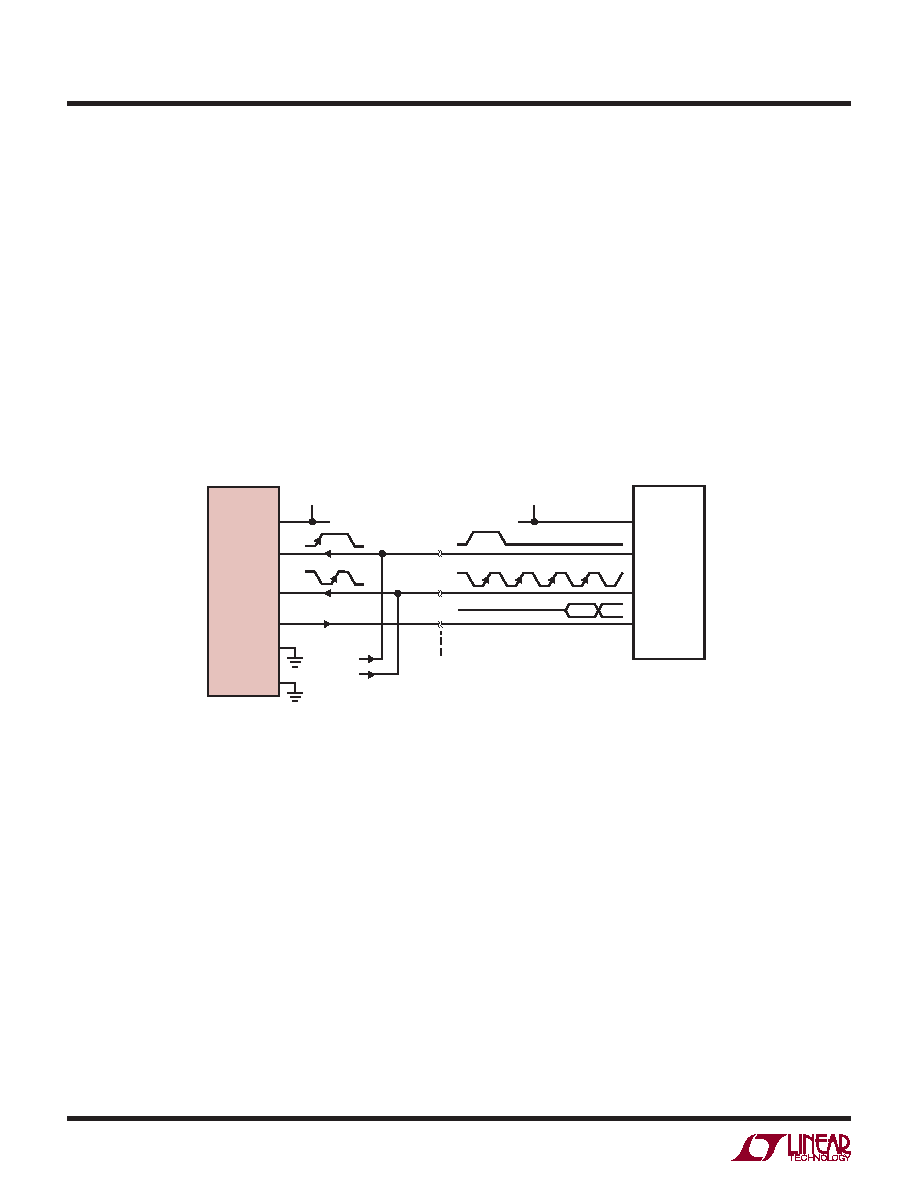
APPLICATIONS INFORMATION
HARDWARE INTERFACE TO TMS320C54x
The LTC2351-14 is a serial output ADC whose interface
has been designed for high speed buffered serial ports in
fast digital signal processors (DSPs). Figure 7 shows an
example of this interface using a TMS320C54X.
The buffered serial port in the TMS320C54x has direct
access to a 2kB segment of memory. The ADC’s serial
data can be collected in two alternating 1kB segments,
in real time, at the full 1.5Msps conversion rate of the
LTC2351-14. The DSP assembly code sets frame sync
mode at the BFSR pin to accept an external positive going
pulse and the serial clock at the BCLKR pin to accept an
external positive edge clock. Buffers near the LTC2351-14
may be added to drive long tracks to the DSP to prevent
corruption of the signal to LTC2351-14. This conguration
is adequate to traverse a typical system board, but source
resistors at the buffer outputs and termination resistors
at the DSP, may be needed to match the characteristic
impedance of very long transmission lines. If you need
to terminate the SDO transmission line, buffer it rst with
one or two 74ACxx gates. The TTL threshold inputs of the
DSP port respond properly to the 3V swing used with the
LTC2351-14.
Figure 7. DSP Serial Interface to TMS320C54x
发布紧急采购,3分钟左右您将得到回复。
相关PDF资料
LTC2355IMSE-14#TRPBF
IC ADC 14BIT 3.5MSPS 10-MSOP
LTC2356IMSE-14#TRPBF
IC ADC 14BIT 3.5MSPS 10-MSOP
LTC2366HTS8#TRPBF
IC ADC 12BIT 3MSPS TSOT23-8
LTC2379HMS-18#PBF
IC ADC 18BIT SPI/SRL 16MSOP
LTC2380HMS-16#TRPBF
IC ADC 16BIT 2MSPS 16-MSOP
LTC2382HMS-16#PBF
IC ADC 16BIT 1CH 500KSPS 16-MSOP
LTC2383HMS-16#PBF
IC ADC 16BIT 1CH 1MSPS 16-MSOP
LTC2393IUK-16#TRPBF
IC ADC 16BIT SER/PAR 1M 48-QFN
相关代理商/技术参数
LTC2351IUH-12#PBF
功能描述:IC ADC 12BIT 1.5MSPS 32-QFN RoHS:是 类别:集成电路 (IC) >> 数据采集 - 模数转换器 系列:- 标准包装:1,000 系列:- 位数:16 采样率(每秒):45k 数据接口:串行 转换器数目:2 功率耗散(最大):315mW 电压电源:模拟和数字 工作温度:0°C ~ 70°C 安装类型:表面贴装 封装/外壳:28-SOIC(0.295",7.50mm 宽) 供应商设备封装:28-SOIC W 包装:带卷 (TR) 输入数目和类型:2 个单端,单极
LTC2351IUH-12#TRPBF
功能描述:IC ADC 12BIT 1.5MSPS 32-QFN RoHS:是 类别:集成电路 (IC) >> 数据采集 - 模数转换器 系列:- 标准包装:1,000 系列:- 位数:16 采样率(每秒):45k 数据接口:串行 转换器数目:2 功率耗散(最大):315mW 电压电源:模拟和数字 工作温度:0°C ~ 70°C 安装类型:表面贴装 封装/外壳:28-SOIC(0.295",7.50mm 宽) 供应商设备封装:28-SOIC W 包装:带卷 (TR) 输入数目和类型:2 个单端,单极
LTC2351IUH-14#PBF
功能描述:IC ADC 14BIT 1.5MSPS 32-QFN RoHS:是 类别:集成电路 (IC) >> 数据采集 - 模数转换器 系列:- 标准包装:1 系列:microPOWER™ 位数:8 采样率(每秒):1M 数据接口:串行,SPI? 转换器数目:1 功率耗散(最大):- 电压电源:模拟和数字 工作温度:-40°C ~ 125°C 安装类型:表面贴装 封装/外壳:24-VFQFN 裸露焊盘 供应商设备封装:24-VQFN 裸露焊盘(4x4) 包装:Digi-Reel® 输入数目和类型:8 个单端,单极 产品目录页面:892 (CN2011-ZH PDF) 其它名称:296-25851-6
LTC2351IUH-14#TRPBF
功能描述:IC ADC 14BIT 1.5MSPS 32-QFN RoHS:是 类别:集成电路 (IC) >> 数据采集 - 模数转换器 系列:- 标准包装:1,000 系列:- 位数:12 采样率(每秒):300k 数据接口:并联 转换器数目:1 功率耗散(最大):75mW 电压电源:单电源 工作温度:0°C ~ 70°C 安装类型:表面贴装 封装/外壳:24-SOIC(0.295",7.50mm 宽) 供应商设备封装:24-SOIC 包装:带卷 (TR) 输入数目和类型:1 个单端,单极;1 个单端,双极
LTC2351IUH-14PBF
制造商:Linear Technology 功能描述:ADC 1.5Msps 14-Bit Serial QFN32EP
LTC2355CMSE-12#PBF
功能描述:IC ADC 12BIT 3.5MSPS 10-MSOP RoHS:是 类别:集成电路 (IC) >> 数据采集 - 模数转换器 系列:- 标准包装:1 系列:microPOWER™ 位数:8 采样率(每秒):1M 数据接口:串行,SPI? 转换器数目:1 功率耗散(最大):- 电压电源:模拟和数字 工作温度:-40°C ~ 125°C 安装类型:表面贴装 封装/外壳:24-VFQFN 裸露焊盘 供应商设备封装:24-VQFN 裸露焊盘(4x4) 包装:Digi-Reel® 输入数目和类型:8 个单端,单极 产品目录页面:892 (CN2011-ZH PDF) 其它名称:296-25851-6
LTC2355CMSE-12#TRPBF
功能描述:IC ADC 12BIT 3.5MSPS 10-MSOP RoHS:是 类别:集成电路 (IC) >> 数据采集 - 模数转换器 系列:- 标准包装:1,000 系列:- 位数:16 采样率(每秒):45k 数据接口:串行 转换器数目:2 功率耗散(最大):315mW 电压电源:模拟和数字 工作温度:0°C ~ 70°C 安装类型:表面贴装 封装/外壳:28-SOIC(0.295",7.50mm 宽) 供应商设备封装:28-SOIC W 包装:带卷 (TR) 输入数目和类型:2 个单端,单极
LTC2355CMSE-14#PBF
功能描述:IC ADC 14BIT 3.5MSPS 10-MSOP RoHS:是 类别:集成电路 (IC) >> 数据采集 - 模数转换器 系列:- 标准包装:1 系列:microPOWER™ 位数:8 采样率(每秒):1M 数据接口:串行,SPI? 转换器数目:1 功率耗散(最大):- 电压电源:模拟和数字 工作温度:-40°C ~ 125°C 安装类型:表面贴装 封装/外壳:24-VFQFN 裸露焊盘 供应商设备封装:24-VQFN 裸露焊盘(4x4) 包装:Digi-Reel® 输入数目和类型:8 个单端,单极 产品目录页面:892 (CN2011-ZH PDF) 其它名称:296-25851-6